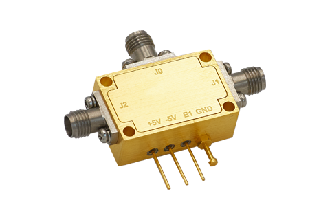
ZTS PIN Diode Switch Introduction
The microwave switch make use of PIN diode to achieve the impedance characteristics of ON or OFF under the forward and reverse bias voltages, and realizes the control of microwave signal conversion.
The DC volt-ampere characteristics of PIN diodes are the same as PN junction diodes, but there are fundamental differences in the microwave frequency band. Since the total charge of the I layer of the PIN diode is mainly generated by the bias current, not by the instantaneous value of the microwave current, it only presents a linear resistance to the microwave signal. The resistance value is determined by the DC bias, the resistance value is small when the forward bias is close to a short circuit, and the resistance value is large when the reverse bias is close to the open circuit.Therefore, the PIN diode does not generate a nonlinear rectification effect on the microwave signal, which is the fundamental difference from the general diode, so it is very suitable for microwave control devices.
Main parameter description:
Insertion loss and isolation:
The PIN diode actually has a certain value of reactance and loss resistance, so the attenuation of the switch is not zero when it is turned on, which is called forward insertion loss, and its attenuation when the switch is off is not infinite, which is called isolation. The two are the main indicators to measure the pros and cons of the switch. Generally, it is hoped that the insertion loss of the switch is small and the isolation is large.
Switching time:
Due to the charge storage effect, it takes a process for the PIN diode to change from off to on state and from on to off state. The time required for this process is the switching time. The pulse control signal is represented by curve A, and the envelope of the controlled microwave pulse is represented by curve B. The "turn-on delay" is the time required from 90% of the control pulse to 10% of the envelope of the controlled microwave pulse. Switch on time" is the time required for the controlled microwave pulse envelope to go from 10% to 90%, also called "rising edge". The "off delay" is the time required for 10% of the control pulse to 90% of the envelope of the controlled microwave pulse, and the "switch off time" is the time required for the envelope of the controlled microwave pulse from 90% to 10%. Called "falling edge" .Generally speaking, "turn-on delay" and "turn-off delay" mainly depend on the driver circuit, while "rising edge" and "falling edge" mainly depend on the choice of PIN diode and bias circuit.
Power capacity:
Under given working conditions, the maximum input power that a microwave switch can withstand. It is related to PIN diode power capacity, circuit type (in series or in parallel), working state (continuous wave or pulse) and heat dissipation conditions. Generally speaking, there are two power damage mechanisms for PIN switches, one is voltage breakdown (common in pulsed power), and the other is thermal burn (common in continuous wave).
VSWR Coefficient:
The VSWR coefficient only reflects the port input and output matching conditions. The VSWR coefficient of the port is the smallest, and the insertion loss of the switch is not necessarily the smallest; but VSWR coefficient of the switch with the smallest insertion loss must be small.
Video leakage:
The direct leakage of modulated video pulses on the main RF line. When the modulation speed of the video pulses is high and the carrier frequency is low, the radio frequency energy of the leaked video may be aliased with the modulated carrier and cannot be filtered by a high-pass filter, resulting in bit errors. , So the smaller the video leak, the better.
Harmonic:
PIN diodes are also non-linear, so harmonics are generated. In broadband applications, PIN switches may fall in the frequency band and cause interference. ZTS Technologies Co., Ltd. can provide you with high-quality low-harmonic PIN switches.
Classification and structure description
Relective and Absorptive
The reflective switch acts as isolation by reflecting the input microwave signal back when the PIN diode is turned on. Therefore, VSWR in the "on" state is better, but VSWR in the "off" state is poor; The absorption switch uses the load to absorb the reflected signal when the PIN diode is turned on, which improved VSWR, so VSWR in the "on" and "off" states is better. Generally, the withstand power of a reflective switch is larger than that of an absorptive switch. From the perspective of engineering applications, although its price is slightly higher, we recommend using an absorptive switch, because it can reduce the inter-stage traction of the system in the off state.
Control mode
The switch adopts TTL signal control, "1" off, "0" on or "1" on and "0" off. Compatible with ECL
Connector type
The connector is mainly SMA series, or removable. The removable switch is a microstrip pin interface after removing the connector seat, which can be easily assembled with the circuit, but at this time, please pay attention to the signal crosstalk in the space to avoid reducing the isolation of the system.


